
Creating interlayered superconducting/insulating van der Waals heterostructures
- Rafal Tekreeti
- Aug 31, 2022
- 2 min read
Updated: Feb 7, 2023
Senior postdoctoral fellow of Research Foundation-Flanders (FWO)
Department of Physics & NANOlab Center of Excellence, University of Antwerp
We have developed a new strategy to create interlayered bulk materials, hosting atomically-thin layers with highly diverse electronic properties – from insulating to superconducting. Collaborating with an experimental group from the National Graphene Institute in Manchester, our quantum mechanical simulations at the atomic scale have shed light on the origin of this diverse behavior.

In 2004, the first atomically-thin two-dimensional (2D) material was created: graphene, a single layer of carbon atoms. This feat yielded the scientists who achieved this, Andre Geim and Konstantin Novoselov from the University of Manchester, the Nobel Prize in Physics in 2010. This major breakthrough in physics and materials science has opened up a whole new research field on 2D materials and their technological applications.
Since that time, many new 2D materials have been discovered. The interactions between these materials are usually mediated by weak van der Waals forces. This enables controlled stacking of different materials into so-called van der Waals heterostructures, enabling the creation of new materials with desired properties by design.
To tackle this intricate many-body problem, we relied on the high-performance computing infrastructure provided by the VSC.
In a recent issue of the journal Nano Letters, we report on the synthesis and characterization of a new van der Waals heterostructure of tantalum disulfide (TaS2). It consists of two alternating layers with distinct crystal structures and physical properties. At higher temperatures, both layer types are simply metallic. However, at low temperatures, one turns into an insulator, while the other becomes superconducting. This implies that the former does not conduct electricity, yet the latter conduct perfectly (without any losses due to resistance).
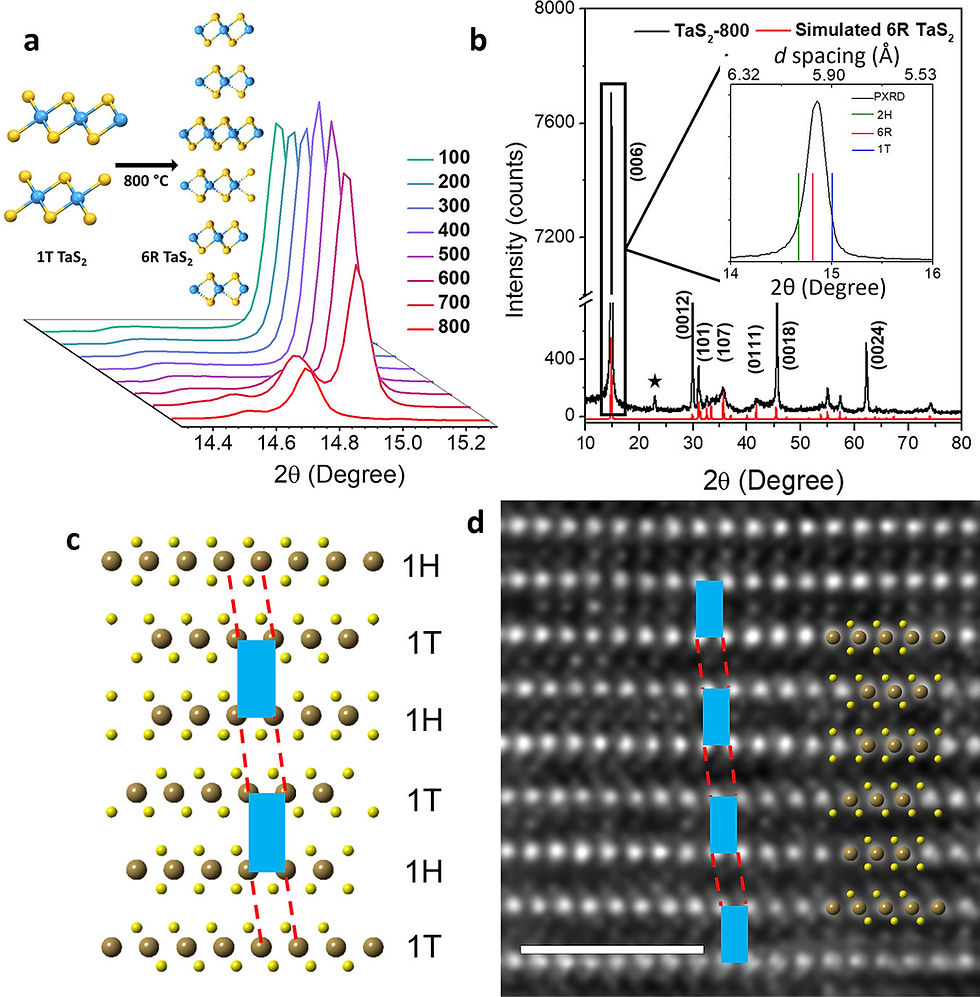
Crystal structure of the 6R-phase of TaS2, consisting of alternating 1T and 1H monolayers, as obtained from scanning transmission electron microscopy (performed by the EMAT group of the University of Antwerp).
To fully understand the origin of this unusual combination of properties, we have theoretically investigated the behavior of the electrons in this material. We used first-principles calculations, rooted in the basic laws of quantum mechanics. The interaction of electrons with quantum lattice vibrations (called phonons) was also taken into account, to describe the emergence of superconductivity. To tackle this intricate many-body problem, we relied on the high-performance computing infrastructure provided by the VSC.
Our calculations have unequivocally proven that the coexistence of superconducting and insulating layers stems directly from the different atomic arrangements in the two-layer types. Its alternating layered structure makes this material a true 2D superconductor in bulk form and opens a plethora of intriguing questions related to the effect of interlayer coupling on the superconducting behavior. Moreover, it exemplifies an entirely new approach to creating junctions of two superconductors separated by a thin insulating layer (so-called Josephson junctions), with important technological applications, such as superconducting qubit devices aimed at quantum computing.
Article: A. Achari, J. Bekaert, et al., “Alternating Superconducting and Charge Density Wave Monolayers within Bulk 6R-TaS2”, in Nano Letters, https://doi.org/10.1021/acs.nanolett.2c01851
Dr. Jonas Bekaert was also our guest at VSC Success Stories, he showcased the importance of VSC's supercomputers in his research to design new ultrathin materials for future #energy #solutions, You can watch his story here